technologies
Microscopic imaging techniques
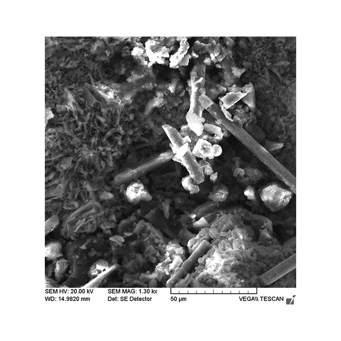
VEGA/SBH Tescan + EDS INCA PentaFET x3 Oxford Instruments
In scanning electron microscopy (SEM), scanning is performed using a focused beam of electrons that interact with atoms on the surface of the sample. The SE detector collects secondary electrons that allow imaging of details of the sample surface topography. The BSE detector detects backscattered electrons so that phase contrast can be obtained. The X-rays emitted when the sample is bombarded with an electron beam are collected by an EDS detector. This allows the elemental composition of the sample to be analysed.
The SEM technology allows detailed analysis of the sample surface topography and composition. Conductive samples can be measured without prior preparation. A metallic conductive layer must first be sputtered or vapourised onto samples that are not conductive.
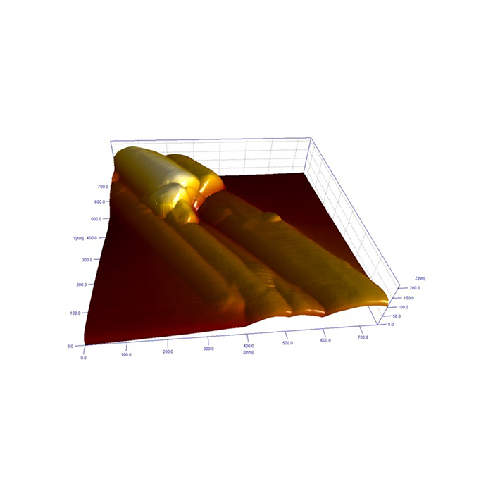
diInnova Bruker
Atomic force microscopy is based on the measurement of local interactions (including van der Waals, electrostatic, magnetic, capillary or ionic repulsion) between the scanning blade and the sample. The measured value is the magnitude of the deflection of the beam with the blade or the amplitude of the probe oscillation. The method of measurement allows the detection of different types of interactions on the sample surface and visualisation in the form of a distribution map.
Measuring capability: topography (roughness), force spectroscopy, lateral forces, phase shift, force-modulated microscopy (FMM), nanoscratching, nanoindentation, Kelvin probe force microscopy (KPFM), electrostatic force microscopy (EFM), scanning tunneling microscopy (STM). The AFM microscopy can be used, among other things, to determine local mechanical properties, analyse roughness or determine coating thickness.
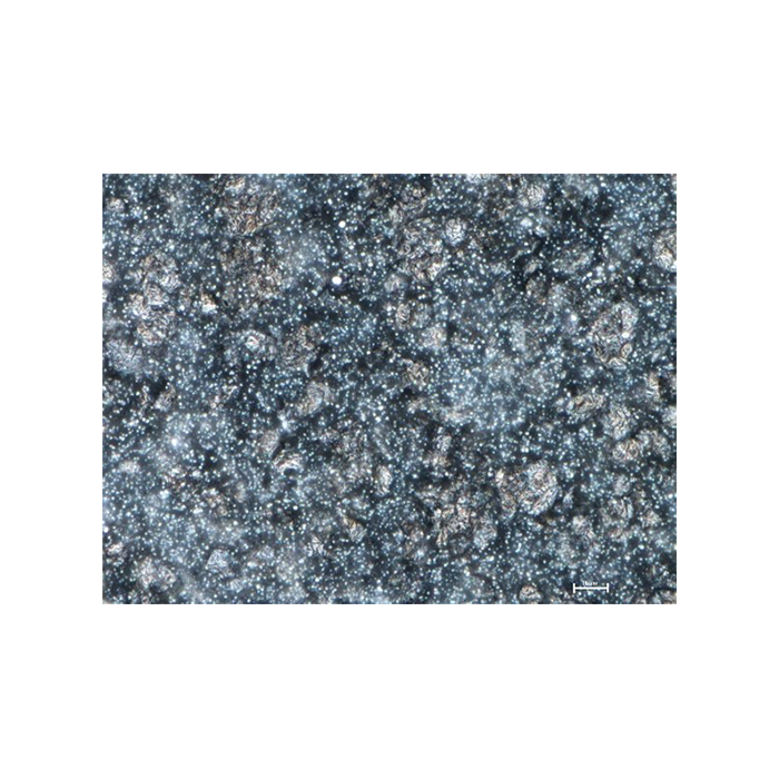
Nikon Eclipse MA200
Optical metallographic microscopy with both brigh tfield and dark field measurement capabilities and Nomarski contrast. The Nomarski differential interference contrast method DIC enables analysis of sample surface topography with nanometre-scale irregularities, makes structures with different refractive indices visible and causes a chiaroscuro effect on the image and an impression of its spatiality. Magnification ranges available include 5, 10, 20, 50 and 100×.


