offer
Technologies
Based on many years of experience, we offer our customers technical advice as well as joint product concept development. We offer and manufacture custom solutions, ranging from small rods and tubes (cores) in the form of tubes made from Al70 high alumina mass to complex components/fittings with complex geometries made by injection moulding from soapstone mass. Depending on the application and operating conditions of the component, we select the most suitable ceramic material with the highest manufacturing quality.
Our products include:
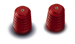
- fittings, single and multi-channel soapstone insulators,
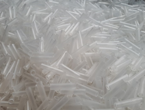
- ceramic cores (tubes) in Al70 with dimensions: OD from 4.0 to 20.0 mm, both single and multi-channel (2, 4 or 6 holes, with custom diameters).
- high alumina centring fittings,
- ceramic adhesives,
- ceramic masses.
Technology for the manufacture of PTFE-coated fibreglass flat insulating sheaths for use in the electrical industry, in particular for insulating thermo-bimetallic plates in small electrical switches, as well as for insulating radiator lead wires.
Formlabs Form 3:
- Low Force Stereolithograpy
- working area: 145 x 145 × 185 mm, layer thickness: 25 – 300 μm, materials: standard and increased strength resins, rubber-like resins with rubber-like properties or dental biocompatible resins.
BCN3D Epsilon W27:
- Fused Deposition Modelling
- working area: 420 × 300 × 220 mm, layer thickness: 50 – 500 μm, materials: ABS, PLA, PET-G thermoplastics
Sinterlit Lisa Pro:
- Selective Laser Sinterling,
- working area: 150 × 200 × 260 mm, layer thickness: 75 – 175 μm, materials: polyamide, nylon, PEEK and others.
Delta WASP 2040 Clay:
- Fused Deposition Modelling
- working area: 200 × 400 mm, layer thickness: 500 – 2000 μm, materials: porcelain, stoneware, clay, etc.
VEGA/SBH Tescan + EDS INCA PentaFET x3 Oxford Instruments
- Scanning electron microscope (SEM) with EDS X-ray microanalysis system
- Operating voltage 5-30 kV (low voltage), maximum available magnification approx. 10,000× (depending on the type of material tested), direct measurement for conductive samples, for non-conductive samples after sputtering of the metallic layer.
diInnova Bruker
- Atomic force microscope (AFM)
- Maximum scanning area 100 × 100 µm, Z-axis scanning range 7 µm, imaging resolution 0.1 nm.
Nikon Eclipse MA200
- Optical microscope with Nomarski DIC contrast metallography
- Magnification available: 5, 10, 20, 50 and 100×, Z-axis image folding, ability to record short videos.
We are able to test new material solutions on a laboratory to semi-technical scale or optimise process parameters for the manufacture of single or multi-component products from unfilled or composite materials. The scale of the technology tests allows new technology assumptions to be verified without having to rearm the production line.
Technologies to be used:
- extrusion lines with water or air cooling of the extrudate
- extrusion lines with extrudate heating
- injection lines
- 30 tonne hydraulic belts with 250°C heated moulds
- gravity and pressure castings
- 3D printing
- pressure mixing, tribological mixing, dispersion, ultrasonic homogenisation
- high-temperature processing furnaces


